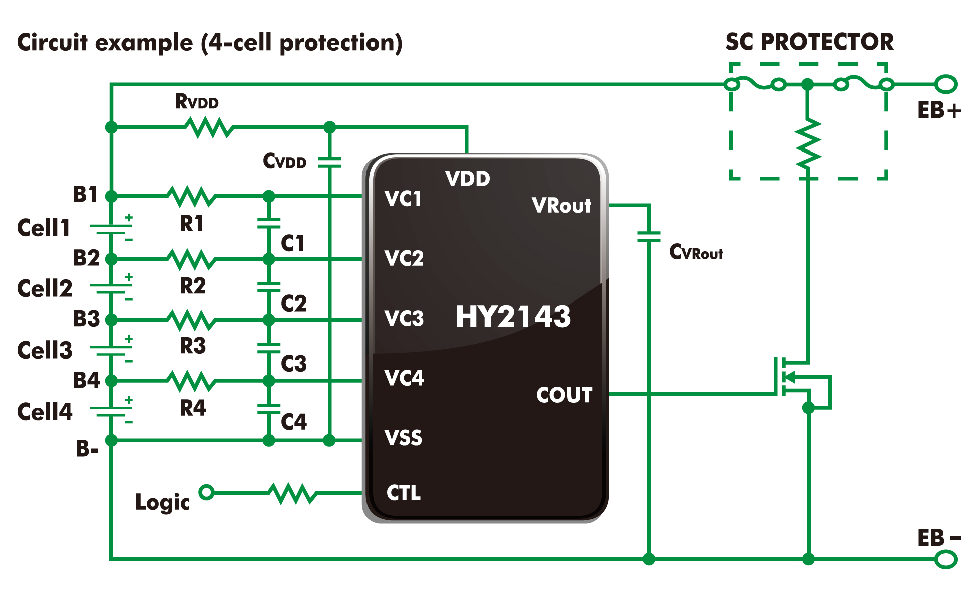
HY2143
HY2143 Series Main Features
- High-accuracy voltage detection circuit
- Delay time is set by internal circuit (external capacitor is not needed)
- Output logic: Active high CMOS output; the high level is 4.7V (typical) output from regulator.
- utput logic active high maximum time: (optional; not-limited as default)
- Low current consumption
- Operation mode 5.0μA typ., 9.0μA max (VCelln = 3.9V).
- Shutdown mode 1: 4.5μA typ., 8.0μA max. (VCelln = 3.1V
- Shutdown mode 2: 0.6μA typ., 1.0μA max. (VCelln = 2.0V,)
- LDO output circuit
- LDO output voltage 3.0V/3.3V typ. Accuracy: ±65mV
- LDO output current 2mA max.
- Input voltage detection level:
- Voltage detection level (from VDD) 2.8V typ. Accuracy: ±1V
- High voltage resistant design: the absolute maximum rated value is 30V.
- Wide operating temperature range: -40°C to +85°C
- Small package: DFN-2.0*2.0-8L
- Halogen free green product
Самые страстные и популярные ролики тут. Скачать любое видео можно бесплатно
Package Type DFN8 (2.0X2.0mm)
| Product Name | Overcharge Detection Voltage VCUn |
Overcharge Release Voltage VCRn |
Shutdown 2 Detection Voltage VSD2n |
Overcharge Detection Delay Time TOCn |
Overcharge Release Delay Time TCRn |
Reset Delay Time of Overcharge Detection Counter TDTR |
LDO Output Voltage VLDO |
Shutdown 2 Detection Delay Time TSD2n |
|---|---|---|---|---|---|---|---|---|
| HY2143-DA1C | 4.500 V | 4.200 V | 2.500 V | 6.0s | 16ms | 6ms | 3.300 V | 6s |
| HY2143-DA1H | 4.500 V | 4.200 V | 2.500 V | 6.0s | 16ms | <0.6ms | 3.000 V | 6s |
| HY2143-EA1D | 4.550 V | 4.250 V | 2.500 V | 6.0s | 16ms | 6ms | 3.000 V | 6s |
| HY2143-FA1H | 4.600 V | 4.300 V | 2.500 V | 6.0s | 16ms | <0.6ms | 3.000 V | 6s |
| HY2143-GA1H | 4.650 V | 4.300 V | 2.500 V | 6.0s | 16ms | 6ms | 3.000 V | 6s |
SelectionGuide