HY310x
Product Features
- Operation voltage: 2.4V to 3.6V
- Temperature range: -40℃ to +85℃
- Built-in VDDA regulator, 2.4V, 2.7V, 3.0V and 3.3V voltage selection
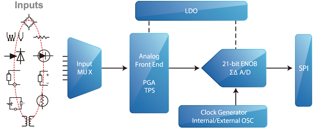
- External/internal clock source
- SPI interface
- Built-in temperature sensor with ±2℃ accuracy
- 16-pin SSOP
- Up to 4 analog channels
- Built-in DC offset input
- 24-bit fully differential ΣΔ analog-to-digital converter (ADC)
- Lowest RMS noise level: 50nV
- Output rate, 10, 80, 640 and 2560SPS selection
- 50/60Hz signal rejection
- Reference input buffer
- Operation current:
- 950μA @ gain=64, 128
- 300μA @ gain=1, 2 or 4
- Built-in PGA, x1, x2, x4…x128 gain amplification
HY310x Series
| Model No. | VDD | Internal Clock |
System Clock |
ADC ENOB |
ADC Gain |
PGA Gain |
Sample Rate |
RMS Noise | TPS | External Crystal |
Serial Interface |
Package |
|---|---|---|---|---|---|---|---|---|---|---|---|---|
| HY3102 | 2.4V~ 3.6V |
320KHZ | 320KHZ | 21-bit x2 | 1~4 | 8~32 | 10sps~ 2560sps |
50nV (10SPS) | Y | – | SPI | SSOP 16 |
| HY3106 | 2.4V~ 3.6V |
320KHZ | 320KHZ~ 4.9152MHZ |
21-bit x4 | 1~4 | 8~32 | 10sps~ 2560sps |
50nV (10SPS) | Y | 4.9152MHZ | SPI | SSOP 16 |
Tool description and software download area